

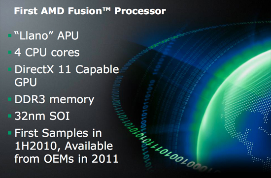
Proto vznikla už před lety pointa, že grafické jádro má svůj specifický a brutální výkon a lze ho využít nejen v pouhopouhém zobrazení a grafice. Fusion je spojení grafického čipu, procesoru a komunikátoru do jendoho pouzdra (čipu). Ovšem to hlavní je, že Fusion nepočítá pouze s náhradou IGP jak ji známe dneska a nebo obdobou Intel Core i5 6xx a i3 5xx, ale že grafický čip bude efektivněji spolupracovat s procesorovou jednotkou přes speciální řadič a zastávat i programovatelné výpočtové operace. Dnes se poodhalila první rouška tajemství a pár informací bylo uveřejněno...První generací Fusion bude pro 1Q 2011 tzv. procesor LIano.
AMD LIano a první Fusion generace....Dovolím si pouze citovat z vybraného webu:
CHIP DESIGNER AMD has been talking up some of the x86 design features for its first Fusion processor at the International Solid State Circuits Conference (ISSCC) in San Francisco this week.
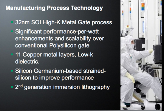
The upcoming 'Llano' Accelerated Processing Unit (APU) will see the joining of a 32nm silicon-on-insulator (SoI) Phenom II quad core CPU with a DirectX 11 capable GPU on the same die. This is a more sophisticated approach than Intel's at present, in which it simply adds a GPU chip to the processor package and calls that 'integrated'.
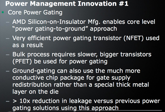
According to AMD senior fellow Samuel Naffziger, the company has focused heavily on cutting power usage in the x86 section of the APU, allowing more juice for the GPU and keeping heat generation and power waste to a minimum.
The SoI approach enables core level power gating-to-ground, thereby allowing the use of NFET transistors rather than the bulkier and more sluggish PFET transistors for power gating while negating the need for a special thick metal layer on the die to handle gate supply redistribution.
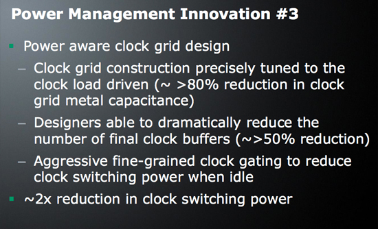
Another major design change by AMD has been the overhaul of the clock grid design, taking the standard fully populated grid and stripping it down to the bare essentials.
Naffziger reckons this has greatly reduced the number of final clock buffers, thereby massively lowering the clock grid metal capacitance and allowing for fine-grained clock gating to reduce clock switching power when idle. He admits that this means that a new grid layout will probably have to become part of the chip design process, but says that the massive power inefficiencies and leakage caused by using a fully populated grid means they are no longer feasible in a Fusion type architecture.
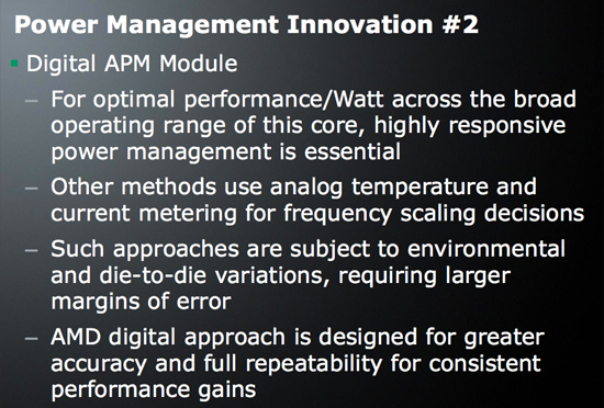
Lastly Chimpzilla has created a digital power management module for keeping tabs on power usage, which it reckons tears strips off the more common analogue temperature and current metering methods used for making frequency scaling decisions, which require larger margins of error due to environmental and die-to-die variations.
The Llano chips are set to start sampling in the first half of 2010 and will only be available to OEMs from early next year, initially being offered on the 'Sabine' platform for notebooks and 'Lynx' for the desktop version. µ
Llano will go up against Sandy Bridge, which seems to have been pushed back to 2011 for volume availability according to Intel’s internal roadmaps. While Sandy Bridge will have graphics on-die, it will still only be DX10 class - AMD will have the feature-set advantage as far as graphics is concerned
http://www.theinquirer.net/inquirer/new ... usion-chip
http://www.anandtech.com/cpuchipsets/sh ... spx?i=3736
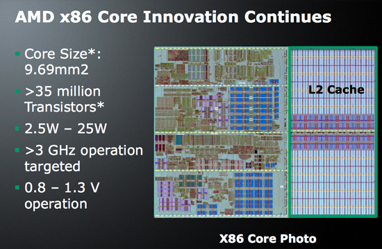
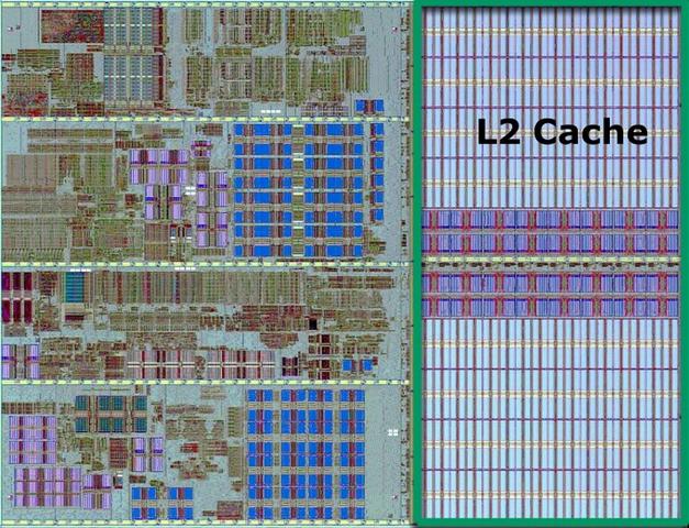
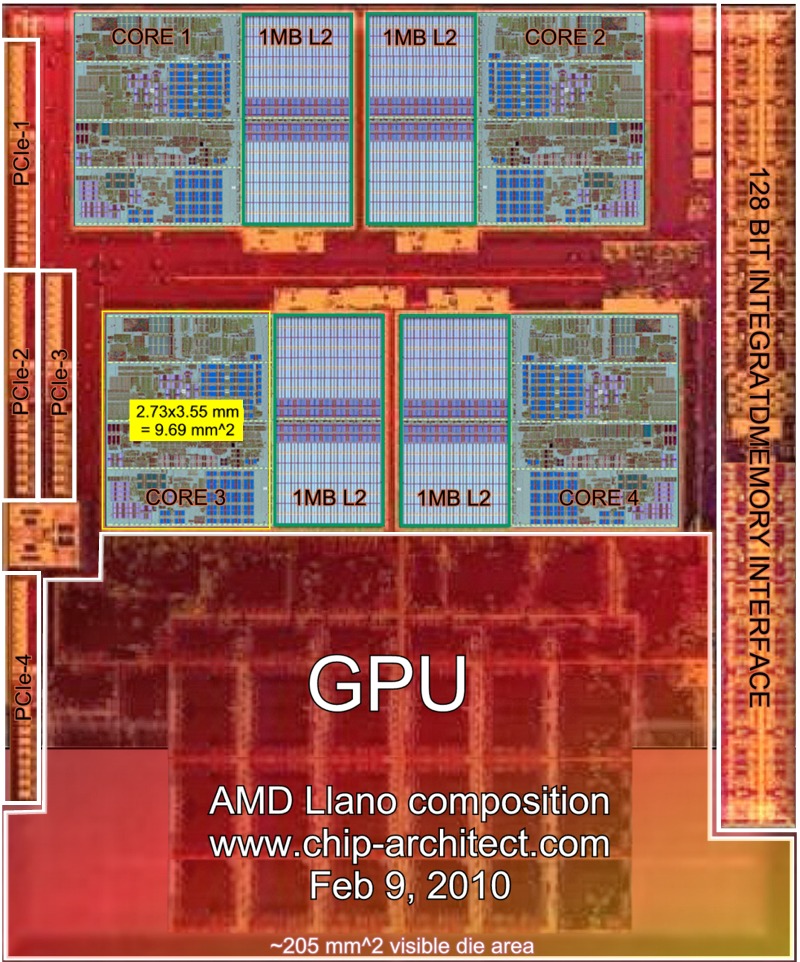
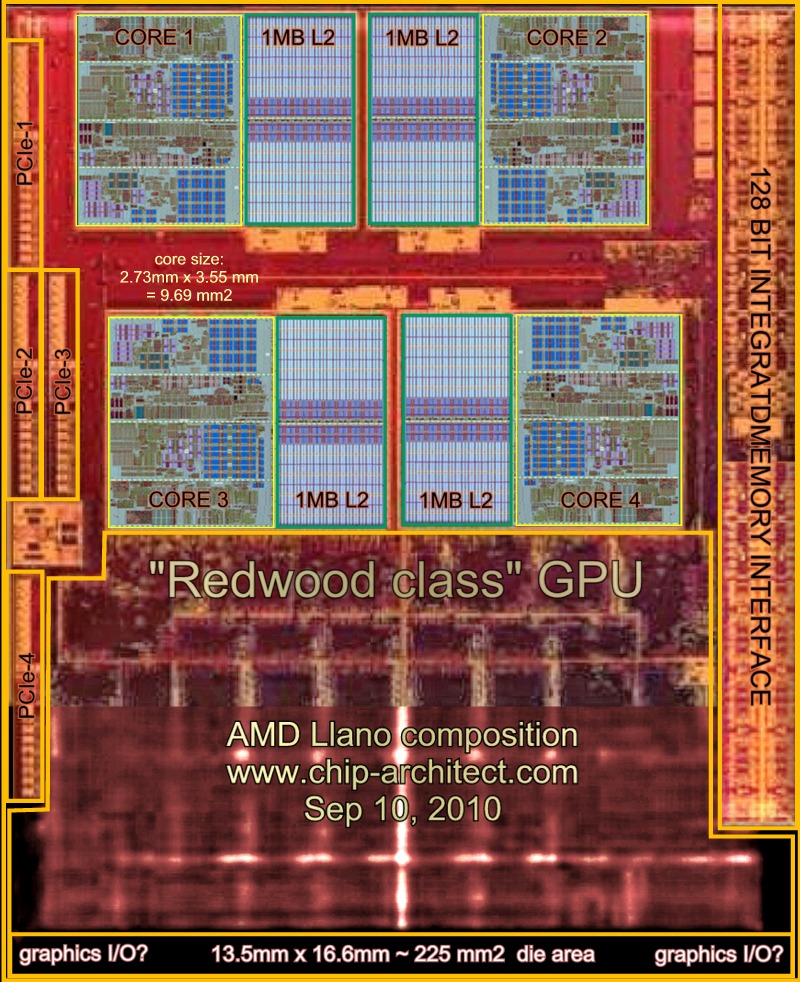
přidán rozbor die LIano
http://chip-architect.com/news/Llano_comp2.jpg


