Re: AMD Vega - Info, spekulace
Napsal: pon 5. lis 2018, 13:15
Diskuze o hardware, software a overclockingu
https://forum.pctuning.cz/
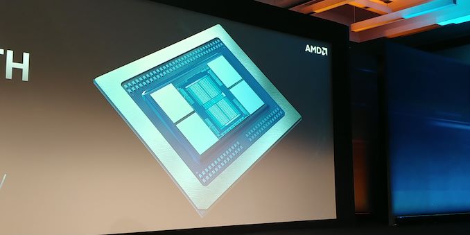
13.2B transistors, 331 mm2
TDP 300W
frekvence 1,8GHz ( turbo ? )
7.4 TGLOPS FP64
14.7 TFLOPS FP32
118 TOPS INT4
One GPU to 16 VMs, or one VM to 8 GPUs
Scale up with multiple GPUs
Many VMs per GPU
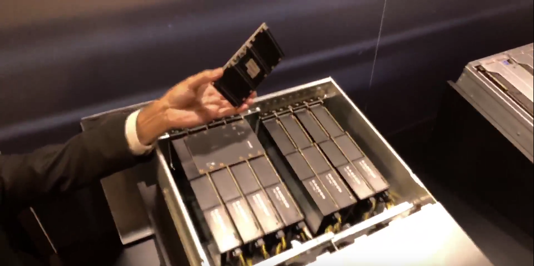
Infinity Fabric GPU to GPU at 100 GB/s per link
64 GB/s Bidirectional CPU to GPU
PCIe 4.0 !
1TB/s bandwidth
32GB of HBM2
end-to-end ECC
Special ML operations for training and inference
50% lower power at same freq
Industry's only hardware-virtualized GPU
Leading edge memory
Flexible Vega architecture
The new AMD Radeon Instinct™ MI60 and MI50 accelerators were designed to efficiently process workloads such as rapidly training complex neural networks, delivering higher levels of floating-point performance, greater efficiencies and new features for datacenter and departmental deployments1.
The AMD Radeon Instinct™ MI60 and MI50 accelerators provide ultra-fast floating-point performance and hyper-fast HBM2 (second-generation High-Bandwidth Memory) with up to 1 TB/s memory bandwidth speeds. They are also the first GPUs capable of supporting next-generation PCIe® 4.02 interconnect, which is up to 2X faster than other x86 CPU-to-GPU interconnect technologies3, and feature AMD Infinity Fabric™ Link GPU interconnect technology that enables GPU-to-GPU communications that are up to 6X faster than PCIe® Gen 3 interconnect speeds4.
Key features of the AMD Radeon Instinct™ MI60 and MI50 accelerators include:
Optimized Deep Learning Operations: Provides flexible mixed-precision FP16, FP32 and INT4/INT8 capabilities to meet growing demand for dynamic and ever-changing workloads, from training complex neural networks to running inference against those trained networks.
World’s Fastest Double Precision PCIe®2 Accelerator5: The AMD Radeon Instinct™ MI60 is the world’s fastest double precision PCIe 4.0 capable accelerator, delivering up to 7.4 TFLOPS peak FP64 performance5 allowing scientists and researchers to more efficiently process HPC applications across a range of industries including life sciences, energy, finance, automotive, aerospace, academics, government, defense and more. The AMD Radeon Instinct™ MI50 delivers up to 6.7 TFLOPS FP64 peak performance1, while providing an efficient, cost-effective solution for a variety of deep learning workloads, as well as enabling high reuse in Virtual Desktop Infrastructure (VDI), Desktop-as-a-Service (DaaS) and cloud environments.
Up to 6X Faster Data Transfer: Two Infinity Fabric™ Links per GPU deliver up to 200 GB/s of peer-to-peer bandwidth – up to 6X faster than PCIe 3.0 alone4 – and enable the connection of up to 4 GPUs in a hive ring configuration (2 hives in 8 GPU servers).
Ultra-Fast HBM2 Memory: The AMD Radeon Instinct™ MI60 provides 32GB of HBM2 Error-correcting code (ECC) memory6, and the Radeon Instinct™ MI50 provides 16GB of HBM2 ECC memory. Both GPUs provide full-chip ECC and Reliability, Accessibility and Serviceability (RAS)7 technologies, which are critical to deliver more accurate compute results for large-scale HPC deployments.
Secure Virtualized Workload Support: AMD MxGPU Technology, the industry’s only hardware-based GPU virtualization solution, which is based on the industry-standard SR-IOV (Single Root I/O Virtualization) technology, makes it difficult for hackers to attack at the hardware level, helping provide security for virtualized cloud deployments.
bohužel je to tak...yuri.cs píše:Frekvence o 300MHz vyssi, TDP 300W... Klasicka Vega.
Ňák slow ne?AMD Infinity Fabric™ Link GPU interconnect technology that enables GPU-to-GPU communications that are up to 6X faster than PCIe® Gen 3 interconnect speeds4
Máš to popsané v té zprávěDOC_ZENITH píše:Ňák slow ne?AMD Infinity Fabric™ Link GPU interconnect technology that enables GPU-to-GPU communications that are up to 6X faster than PCIe® Gen 3 interconnect speeds4
Na 300GB/s s NVLink 2.0 to sice nemá, ale furt lepší jak nicPrevious Gen Radeon Instinct compute GPU cards are based on PCIe Gen 3.0 providing up to 32 GB/s peak theoretical transport rate bandwidth performance.
Peak theoretical transport rate performance is calculated by Baud Rate * width in bytes * # directions = GB/s per card
PCIe Gen3: 8 * 2 * 2 = 32 GB/s
PCIe Gen4: 16 * 2 * 2 = 64 GB/s
Vega20 to Vega20 xGMI = 25 * 2 * 2 = 100 GB/s * 2 links per GPU = 200 GB/s
xGMI (also known as Infinity Fabric Link) vs. PCIe Gen3: 200/32 = 6.25x
to má být vtip nebo jen trolíš ???Comby píše:Tu je celkom kvalitný snímok, vie niekto spočítať veľkosť Vega 20 na 7nm?
https://youtu.be/_UevWqz1je4?t=49
hlavně máš to postnuté v tomto vlákně hned nad svým příspěvkem. Už od včerejškaComby píše:Už som si to dohľadal.
Vega 20 je o 45% menší než Vega 10. Jádro o velikosti 332mm2 dosahuje cca 68% plochy Vegy 10 výraběné 14nm Fin Fet procesem-The total number of transistors of Vega 7 nm to be mounted is 13.2 billion and the die size is 332 mm 2 . As Vega 10 manufactured using the 14 nm process technology sequentially has 12.5 billion and 486 mm 2 , the number of transistors has increased by about 6%, while the die size is reduced to about 68%.
takty (max boost clock) jsou o 20% vyšší jak u Vegy 10.I was able to ask. Using this formula, back calculation from the theoretical performance value of 14.7 TFLOPS, the boost maximum clock of Vega 7 nm should be around 1794 MHz. I think that about 16% higher clocking compared to 1546 MHz of Vega 10 is a convincing figure as a result of miniaturization of manufacturing process technology.
Historicky, vždy keď niekto prehlasoval takéto rádové zlepšenia (150x?) tak to bol vždy nejaký scam. Skutočne tam merajú to isté? Fyzicky v tých serdes určite taký rozdiel nieje.Krteq píše:Ještě k tomu xGMI aka Infiniti Fabric Linku
Sice dosahuje o 100GB/s nižší propustnosti jak poslední konkurenční řešení , ale latence jsou řádově nižší
xGMI - 60-70ns
nVLink 2.0 - 10µs
Více - AMD Radeon Instinct MI60 Session 5 Nov 6 2018 Next Horizon (YouTube)
Tie parametre sedia skôr na TSMC10 proces, nie na TSMC7.del42sa píše:Vega 20 je o 45% menší než Vega 10. Jádro o velikosti 332mm2 dosahuje cca 68% plochy Vegy 10 výraběné 14nm Fin Fet procesem-
takty (max boost clock) jsou o 20% vyšší jak u Vegy 10.
https://translate.google.com/translate? ... edit-text=